2 Power management
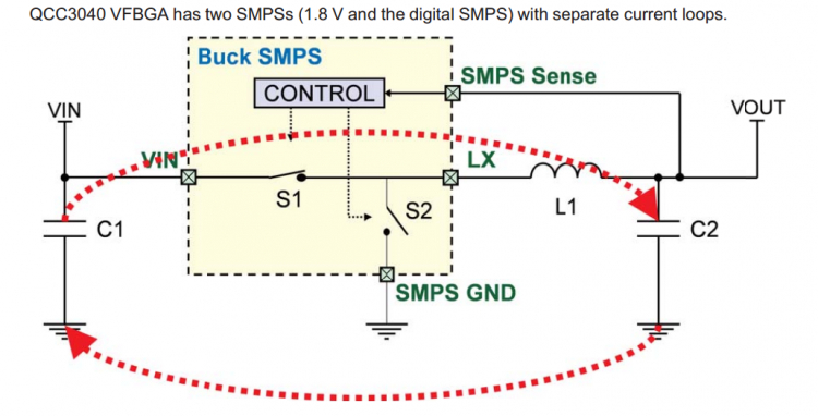
2.1 SMPS
2.1.1 Components specification
2.1.2 Input power supply selection 9
2.1.3 Minimize SMPS EMI emissions
2.1.4 Internal LDOs and digital core decoupling
2.1.5 Powering external components
2.2 Charger
2.2.1 Charger connections.
2.2.2 General charger operation
2.2.3 Temperature measurement during charging
2.3 SYS_CTRL
3 Bluetooth radio
3.1 RF PSU component choice
3.2 RF band-pass filter
3.3 Layout
4 Audio
4.1 Audio bypass capacitors
4.2 Earphone speaker output
4.3 Line/Mic input
4.4 Headphone output optimizition
5 LED pads
5.1 LED driver
5.2 Digital/Button input
5.3 Analog input
5.4 Disabled
6 Reset pin (Reset#)
7 USB interfaces
7.1 USB device port
7.1.1 USB device port
7.1.2 Layout notes
7.1.3 USB charger detection
A QCC3040 VFBGA example schematic and BOM
B Recommended SMPS components specification
B.1 Inductor specifition
B.2 Recommended inductors
B.3 SMPS capacitor specifition


